


Key Takeaways
- ₹1.25 lakh crore approved under India Semiconductor Mission 2.0
- Cabinet approval pending for final implementation decision
- 12 semiconductor projects approved in the first phase
India has advanced its semiconductor expansion plans after the Finance Ministry’s Expenditure Finance Committee approved a ₹1.25 lakh crore outlay under India Semiconductor Mission 2.0. The proposal will now move to the Union Cabinet for final approval and is aimed at strengthening domestic chip manufacturing and design capabilities.
Semiconductor Mission 2.0 Expands Domestic Chip Ecosystem
The proposed allocation under India Semiconductor Mission 2.0 is significantly higher than the ₹76,000 crore committed under the first phase of the mission. The increase reflects a stronger focus on building a complete semiconductor value chain within India, covering fabrication, packaging, equipment, materials, and design capabilities.
The initiative is designed to reduce import dependence and strengthen domestic production capacity in critical semiconductor technologies. It also aims to encourage innovation, support intellectual property creation, and attract global ecosystem participation in India’s semiconductor sector.
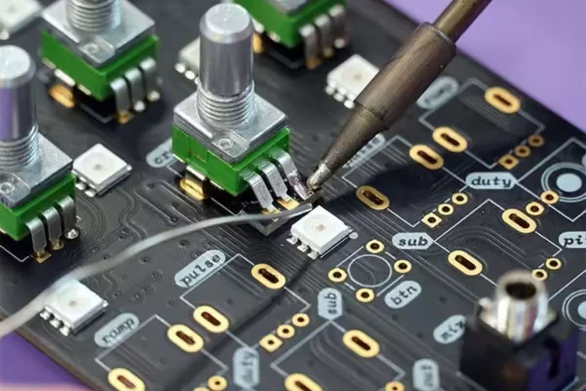
Under the first phase of the mission, the government has approved 12 semiconductor manufacturing projects with a total investment of approximately ₹1.64 lakh crore. These include fabrication units, compound semiconductor facilities, and packaging and assembly plants.
Design And Manufacturing Ecosystem Strengthens
Alongside manufacturing expansion, the government has increased support for semiconductor design through the Design Linked Incentive scheme. A total of 24 projects are currently supported under this scheme to accelerate chip design and development.
In addition, 105 companies have been granted access to advanced chip design tools, improving development capability across the ecosystem and supporting faster innovation cycles.
Official data shows that 23 chip tapeouts have been completed across various semiconductor foundries, including advanced technology nodes. These milestones reflect steady progress in domestic design capability and movement toward production readiness.
Government officials have indicated that the sector is shifting from planning to execution, with early-stage manufacturing activity beginning to take shape. Additional projects are expected to be announced as the ecosystem develops further.
Execution Phase To Drive Next Stage Growth
India Semiconductor Mission 2.0 is focused on building a self-reliant semiconductor ecosystem by integrating fabrication, packaging, design, and supply chain development into a unified structure.
With Cabinet approval pending, the next phase is expected to focus on execution, capacity expansion, and scaling of approved semiconductor projects across the country.
Read the latest articles and success stories on Business Viewpoint Magazine.